The Metal-Oxide-Semiconductor Capacitor As The Fundamental Sensor Element Of A Digital Radiography System
©
By
ROBERT PAUL KING, JR.
A Thesis Presented to the Graduate School of the University of Florida in Partial
Fulfillment of the Requirements for the Degree of
Master of Science
University of Florida
Chairperson: Alan M. Jacobs
Major Department: Nuclear Engineering Sciences
Acknowledgements
This work was made possible by funding from General Imaging Corporation and the U. S. Air Force, and for this I wish to express sincere appreciation. In addition, I would like to thank Dr. Alan Jacobs, my thesis advisor, for creating a situation such that I am able to be involved with a project as stimulating and rewarding as this one and for his guidance and intellectual support during this work. Also, I wish to thank Dr. John Cox, Dr. Robert Fox, and Dr. William Eisenstadt for their continuing guidance and advice during this work.
Abstract
The suitability of the metal-oxide-semiconductor (MOS) capacitor for use in radiography, especially medical radiography, is investigated. Radiography and the parameters of a radiographic sensor are described. The quantum limitation on radiography is described and exposure limitations are used to justify a square sensor element with side length of 100 μm. Due to the biological hazards associated with ionizing radiation, the requirement is adopted for medical radiography that each x-ray photon give rise to a detectable response in the sensor. A sensor element made of a MOS capacitor and phosphor is described. Bounds on expected phosphor performance are justified. The MOS capacitor structure, materials, and operation are described. A test structure MOS capacitor is used to evaluate the suitability of the MOS capacitor for use in a radiography sensor element.
Mathematical techniques for characterizing a MOS capacitor are described. A method is developed for calculating a MOS capacitor's quantum efficiency. This method includes a correction for thermal charge generation. The latitude (i.e. maximum permissible exposure) of the described sensor element is calculated to be well in excess of the requirements of medical radiography. The quantum efficiency of an oversized (330 μm side square) MOS capacitor is determined to be 7% for optical photons of wavelength 540 nm. This wavelength was chosen for measurement based upon phosphor emission spectra. Using the best and worst case phosphor performance, the number of expected charges per x-ray photon was calculated. To detect the influence of a single x-ray photon, readout circuits must resolve a charge packet containing between 83 and 109 electrons. This is a very small charge and will likely not be resolvable within the constraints of this sensor. The measured quantum efficiency is unusually small and possible techniques to improve this value are described.
To correct the quantum efficiency measurement for thermal generation, the thermal generation properties of the MOS capacitor were measured. Thermal generation was observed to be unusually slow with the MOS capacitor taking 50 minutes to equilibrate at room temperature in the dark.
Chapter 1
INTRODUCTION
The research reported here was conducted as part of an ongoing effort to develop a large scale, solid state electronic device for use as a digital sensor in both medical and industrial radiography. Though this work is pertinent to both applications, emphasis is given to medical radiography.
The starting point for this research is the work reported by Jacobs1. It was shown that through the use of multiple stepped exposures and additive image reconstruction, a bare dynamic random-access memory (DRAM) integrated circuit (IC) can be used to acquire high quality, small scale, digital, radiographic images. The architecture of a DRAM makes it awkward to use for radiography. Large radiation exposures and acquisition times are required. Large radiation exposures and acquisition times are unacceptable in medical radiography. In addition, accumulated radiation exposure limits the useful lifetime of a DRAM, thus large exposures are unacceptable for such a device in an industrial environment. High sensitivity is a requirement for both an industrial and a medical, solid-state, radiographic sensor. The bare DRAM is not an acceptable image sensor in either application. In addition to operational and survivability problems, the DRAM architecture is such that it is not feasible to attempt to scale it up to a large size (e.g. 11" x 14").
A more appropriate architecture than that of a DRAM must be developed for use in an electronic radiography sensor. A suitable architecture will use digitization of photogenerated charge acquired during a single exposure. Such an architecture must be based around some electronic device which functions as the fundamental sensor element. The metal-oxide-semiconductor (MOS) capacitor is the fundamental charge storage element in a DRAM and the fundamental sensor element in a charge-coupled-device (CCD). It is well suited to large scale device fabrication. Therefore, it seems a likely first candidate for investigation. The object of this research is to investigate the MOS capacitor for use as the fundamental sensor element in a digital radiography system. The objectives are to model the device's performance as a sensor element and to evaluate its suitability for this task.
Chapter 2 examines the radiography process. It evaluates the objectives of radiography, its inherent limitations, and the role of the radiographic sensor. The performance parameters of interest are discussed, performance goals are defined for medical radiography, and some assumptions about operating conditions are established.
Chapter 3 discusses the MOS capacitor. Its structure, materials, and mechanisms of charge generation and transport are considered.
Chapter 4 discusses the use of the MOS capacitor in radiography. A proposed sensor element geometry is described. Two possible phosphor capabilities are described and justified for use as the best and worst case of an achievable phosphor capability. Expected performance parameters are determined and criteria for medical use are calculated. Issues pertaining to signal readout and processing are described, an expected response to imaging parameters is discussed, and the implications of radiation damage are briefly introduced. The issue of radiation damage has been addressed by other investigators1. Its action is to degrade the performance of the MOS capacitor as well as other electronic components ultimately leading to device failure. A DRAM is sufficiently robust to radiation exposure that interest in a solid state image sensor has not been discouraged. The issues of electronic radiation damage and its implications to system performance and survivability are not closed and deserve additional consideration in later work. They do not receive that consideration here. The interest here is focused on the performance of the unirradiated MOS capacitor and not how that performance degrades with exposure.
Chapter 5 discusses an IC which contains MOS capacitors which were used for investigation. In addition, other devices which were used for data collection are described.
Chapter 6 discusses the methods used to characterize a MOS capacitor. A model of thermal charge generation is described and a model of charge generation under illumination is proposed. A technique of calculating thermal charge generation parameters is described, as are methods of calculating total charge generation rates. A method for calculating the quantum efficiency (efficiency for converting optical photons to charge carriers) is described.
Chapter 7 reports the characteristics of sample MOS capacitors fabricated using the Metal Oxide Semiconductor Implementation Service (MOSIS). The doping profiles of n-type and p-type MOS capacitors are determined and a preference for n-type MOS capacitors is tentatively established and justified. The thermal generation parameters of an n-type MOS capacitor are calculated and reported. The latitude of the test IC MOS capacitor is determined and compared to the latitude requirements for medical radiography. The absolute quantum conversion efficiency of an n-type MOS capacitor at the optical wavelength of interest (540 nm) is calculated and shown to be constant during an exposure cycle.
Chapter 8 investigates the implications of the MOS capacitor's characteristics on its use in medical radiography. The requirements which they place on readout circuitry is determined. Suggested directions for further work are then outlined.
Chapter 2
THE DIGITAL RADIOGRAPHY PROCESS
Radiography
When an object of unknown composition and internal structure is illuminated by a beam of penetrating radiation whose properties are known, properties of the radiation which exits the object can be measured to draw conclusions about the composition and structure of the object. If the objective of this process is to learn how materials are distributed in the object, then this process is known as radiography.
Image Formation
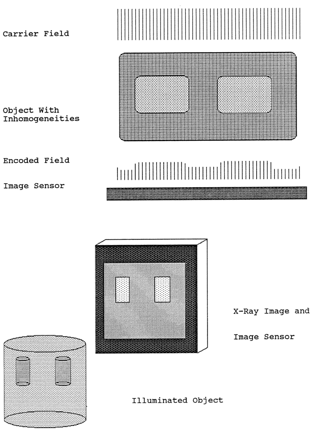
In radiography, information about the composition of the object is encoded on the properties of the carrier beam. By possessing knowledge about the encoding processes and the carrier beam, it is possible to decode information about the object from measured properties of the emerging radiation. As a practical matter, measuring the properties of the emerging radiation is not trivial and therefore every effort is made to keep the properties of the illuminating beam as simple as possible so that the required decoding is minimized. As an example, consider the following simple case. Suppose that to image an object which has x, y, and z dimensions, it is illuminated by a beam of uniform flux, I, from the -z direction. If the quanta of the illuminating beam are monodirectional and monoenergetic, the beam has planar symmetry (i.e. no variation in intensity along the x and y directions), and only the uncollided emerging flux (ΦO) is measured, then the two dimensional information which is encoded on the magnitude of the uncollided flux is the two dimensional distribution of transmission factors, e-P(x,y) as described by Equation 2-1. P(x,y) is the optical path length of the object at (x,y). Figure 2-1 illustrates this situation.
Note that the spatial variation of the uncollided flux is an incomplete description of the emerging beam. As such, it provides only incomplete information about the object. A complete description of the object at location (x,y) would tell what the range of z for the object is at (x,y), what material elements are located there, and how they are distributed along z. The optical path length has this information integrated together as shown in Equation 2-2.
The simple form of radiography described here is the most common. The beam geometry is approximated by using a very small source of radiation which is located much further from the object than the distance between the object and sensor. Non-monochromatic radiation such as that produced by a bremsstrahlung source of x-ray illumination is often used. This results in an averaging process over the energy-dependent interaction coefficients. Sometimes, a non-planar, non-uniform illuminating beam is used so that when the object information is encoded on it, the image will have properties useful for the application. For example, a beam with spherical symmetry can be used to obtain magnification in two dimensions. This effect is unavoidable when the distance between the object and the sensor is not negligible in comparison to the distance between the source and the object. A beam with cylindrical symmetry can be used to obtain magnification in only one dimension. Though this is not common, it would be a consideration in performing transmission radiography with a collimated detector and a line source. In addition, a planar beam can be made non-uniform to allow meaningful and simultaneous imaging of optically thick and thin objects. An example of this is the use of the bowtie filter in CT imaging.
In transmission radiography, no attempt is usually made to detect and interpret scattered radiation, and all the object information which it carries is wasted. Instead, great efforts are made to prevent scattered radiation from reaching the image sensor. Any scattered radiation which is detected by the image sensor contributes undesired information to the image. This undesired information mimics image noise.
Image Sensing
As the beam exits the object, it must be intercepted by an image sensor which is able to measure the uncollided flux and its spatial variation with x and y. Unfortunately, it is not always a simple matter to isolate the uncollided from the scattered flux or distinguish between them. The function of the image sensor is to provide a two dimensional signal, S(x,y) (i.e. a change in some measurable property of the sensor which can vary across its lateral dimensions) in response to the uncollided flux which reaches it. In radiography, any rejection of scatter generally occurs in devices external to the sensor since the sensor's response is a function of the total angular-integrated flux which reaches it. Since conventional radiography sensors typically provide only a time-integrated, energy-weighted signal, the sensor's response is a function of the energy fluence (exposure) which is incident on it. Metal halide film is the most commonly used radiography sensor. It changes its opacity (optical density) in response to the energy fluence which is incident on it. In the medical environment, radiographic film is commonly used with one or more layers of scintillating material placed in contact with it. This is done to improve the film's ability to intercept x-ray photons and to increase the response of the film to x-ray photons which are intercepted. In the medical environment, this is necessary to minimize the patient dose required to obtain a diagnostic quality image. In the industrial environment, lead intensifying screens are more common and are used to reduce the time required to acquire an image of sufficient quality.
Digital Radiography
If the image sensor is intentionally discretized both spatially and in its response variable, it is said to be a digital radiography sensor. Radiography is performed with fields of radiation made up of discrete quanta. These quanta undergo binary interactions (Compton scatter and photoelectric absorption being the most important) in the object to form the x-ray image. The emerging quanta are detected individually by the image sensor to form the recorded image. Though not necessarily digital, all radiography is inherently discrete. In this discussion, a digital radiography sensor refers to an array of sensor elements each of which is capable of absorbing an x-ray photon and converting it to a packet of stored charges. Such a sensor must also have some sort of automatic readout mechanism which is able to prepare an electronic image in a format suitable for a digital computer.
Medical Radiography
The process of forming a medical radiograph involves the interplay of two potential hazards. Ionizing radiation causes damage in biological systems. The most significant form of damage at the exposure levels of interest is genetic damage which can lead to long term, life threatening conditions. However, insufficient or misleading image information can lead to improper medical treatment and present immediate hazards to a patient. Therefore, every effort must be made to extract the maximum possible information from the minimum possible exposure in a diagnostic examination. This means two things. Every effort must be made to absorb each useful x-ray photon which has passed through the patient. In addition, each x-ray photon which is absorbed must give rise to a significant change in the radiographic sensor. For digital imaging, the charge generated by an x-ray photon absorbed in a pixel must correspond to a resolvable grey level for that pixel.
Radiation Source
To exploit the different energy dependencies of the interaction probabilities of body constituents, filtered bremsstrahlung x-ray sources are used which have controllable peak energies. Typically, diagnostic exams use peak energies between 50 and 120 kev. To achieve acceptable contrast, mammographic x-ray spectra typically have peak energies between 30 and 50 keV. Teletherapy portal imaging is forced to use much higher peak energies with the result of very poor primary contrast and scatter rejection. Portal imaging and mammography are special radiographic problems and immediate consideration is limited to the case of general radiography.
In later chapters it is necessary to perform calculations which depend on the energy of an x-ray photon. Calculations based upon energy spectra are complicated to perform. Meaningful calculations based upon energy spectra require a detailed estimate of the x-ray spectrum to be used. In addition, x-ray spectra differ from one x-ray source to another and from one examination to another. Therefore, it is either necessary to perform calculations based upon many different spectra or base calculations on some sort of average spectrum or a simplifying assumption. For this work, a monoenergetic beam of 40 keV photons is taken as representative of an average beam used in diagnostic radiography. Since it does not describe any actual diagnostic x-ray beam, this approximation introduces some errors. However, the average peak energy lies somewhere in the range listed, the average energy in a spectrum lies below its peak, and imaging beams are hardened before they reach the sensor. Therefore this is a reasonable approximation.
Logarithmic Detection
Metal halide film was the first and remains the most popular radiography sensor. Microscopic grains in a piece of radiographic film change their state and become optically opaque as they are exposed. Therefore, radiographic film records image information by darkening in response to exposure. As film grains are exposed, they are no longer available to be exposed and film sensitivity (rate of darkening with respect to incident flux) declines linearly with accumulated exposure. Due to this, the darkness of an area of radiographic film is approximately proportional to the logarithm of the exposure and is thus linearly proportional to P(x,y), the optical path length. This proportionality does not hold for very small exposures and ceases to hold for very large exposures as the film saturates. Radiographic film was not developed to record P(x,y) and it is not obvious that P(x,y) is the description of the body which is most clinically relevant or useful.
It is also not obvious that a sensor element developed for used as a radiography sensor will record P(x,y). In fact, unless the physics of operation are similar, P(x,y) is not expected to be recorded. If the sensor provides a response which is proportional to accumulated exposure (similar to an integrating Anger camera), the relationship between its response and the object optical path length is expected to be greater than linear. In other words, if a sensor does not lose its sensitivity during an exposure, it will be more sensitive to large exposures than a sensor which does. In such a case, the plot of response against optical path length has a positive second derivative and its shape is similar to that of a parabola. When S(x,y) (the response of the sensor at a given position) is plotted against P(x,y) (the optical path length at a given position), the resulting graph is known as a Hurter and Driffield (H&D) Plot. If P(x,y) is the description of the object which is of interest, an electronic image can be processed to yield a linear H&D Plot.
Photon Stopping and Amplification
Radiographic film is virtually transparent to x-rays and any x-ray which interacts with it produces a very small response. Since medical radiography must get the greatest possible information for the smallest possible exposure, steps are taken to improve the cross section and response of film to x-rays. Rare earth salt screens are often placed in close contact with film to absorb the x-rays, create optical photons and transmit those optical photons to the film. The screen's ability to absorb x-ray photons is primarily governed by its thickness. Since light photons spread in the phosphor, screens blur the image that they form and obscure fine detail. A graph of the intensity of a sensor's response against the spatial frequency of the object is known as a modulation transfer function (MTF). The spatial distribution of a sensor's response to a single x-ray photon is known as its point-spread-function (PSF). The PSF and MTF are related by the Fourier transform. To say that an intensifying phosphor tends to obscure fine detail is equivalent to saying that its MTF takes on low values for high spatial frequencies. Such a device is known as a low-pass spatial filter. An intensifying phosphor is a low-pass filter and as such attenuates high-frequency image information and high-frequency image noise. Other means of increasing the film's response to x-rays which are absorbed include increasing the grain size and increasing the development time. These also act at the expense of the MTF. A compromise between a wide-band MTF and high sensitivity must be made in designing an image sensor.
Electronic systems are more flexible than radiographic film. Once a film is exposed and developed, it is very difficult to enhance its appearance and a film which is too light or too dark must be repeated. The first film is discarded and the radiation dose absorbed by the patient during the first exposure is wasted. In contrast, it is a relatively simple matter to apply gain to an electronic signal or multiply the contents of a computer register by a constant. For an electronic image, it need not be a consideration that the information available cannot be seen because the film is too light or too dark. Using window and level controls, any amount of image information can be presented in a viewable form. Of course, amplification cannot provide image information which was not acquired by the sensor. Good sensor performance is still required and a sensor which is completely saturated during an exposure still relays no information.
Resolution and Contrast
As described above, enhancing the sensor's ability to absorb x-ray photons is done at the expense of spatial resolution. In addition, the greatest possible image information must be extracted using the smallest possible exposure, i.e. the smallest possible number of photons. To extract all available image information, each x-ray photon which is absorbed by the screen must be made to independently contribute to the image. In other words, the information/exposure tradeoff is optimized in a detector which can detect individual x-ray photons. The finite number of quanta used to form an image has associated with it a limited ability to statistically resolve spatial detail and contrast. The sensor's sensitivity is optimized by causing it to absorb the maximum number of incident x-ray photons. For radiographic film, spatial resolution requirements directly limit the phosphor thickness which can be used. Since the PSF of the phosphor can be deconvolved from images acquired in a digital format, phosphor thickness is less constrained in digital radiography.
The immediate objective in trying to develop a digital, medical radiography sensor must be to determine what information density is available in a typical medical radiograph and thus what sensor parameters must be met. The available exposure at the sensor is variable not only across the sensor but between different image acquisitions. For this work, the value of 500 μR is chosen to be representative of an average exposure at the sensor for an average medical radiograph. Assuming that only 40 keV photons are used, a photon fluence of 10.9x10⁶ photons/cm2 is calculated to be incident at the image sensori. This photon density can carry an information equivalent between that of the light available outdoors at twilight and the light available under typical indoor room lightingii (based on certain photographic assumptions) .
Consider a square region (pixel) in the image sensor whose side length is d. This region of the sensor intercepts an elemental area, d2, of the x-ray image field. This area is illuminated by an average number of photons, n, given by the average photon density calculated above and the size of the elemental area. Variations in the actual number of photons seen in a given elemental area provide the image information. However, the random nature of radiation generation and interactions, also creates variations in the actual number of photons absorbed in a pixel.
The reason for choosing a small pixel size is to allow imaging of small object details or correspondingly to allow the imaging of high spatial frequency information. The pixel size must be chosen to be sufficiently small to see the smallest image detail which is available to it. However, there are performance trade-offs associated with making the pixels small and thus they must be made as large as the imaging process will allow.
Suppose it is desired to visualize a minimally resolvable image detail. As the problem is outlined above, this image detail should occupy a single pixel. This image detail's photon density has a relative difference, C, with respect to the photon density of the surrounding area. C is the detail's contrast and it takes on values between zero and one. In order to tell an image detail from a statistical fluctuation, the photon density in the pixel must be statistically significantly different from the background photon density. High contrast details are easier to image than low contrast details and thus can be smaller and still be statistically significant. The real issue is the total differential number of photons stopped by the object detail. A high contrast image detail needs less area to stop a given number of photons. A large detail can be lower contrast and still stop a given number of photons. If the total photon density increases, lower contrast and smaller details can stop that same number of photons. This is represented in Equation 2-3 which is derived by Rose3.
The square root is due to the Poisson nature of the process being considered. The five in the denominator on the right hand side dictates the reliability with which it is possible to visualize the image detail and refers to five standard deviations from the mean or a signal-to-noise ratio (S/N) of five. Though not an absolute number, Rose makes arguments for use of five as the threshold S/N for a minimally detectable image feature.
If it is desired to resolve 128 shades of grey (a seven bit image) in a medical image made at an exposure of 500 μR then Equation 2-3 implies that the size of the minimally resolvable x-ray picture element has a side length of 194 μm i.e. the inherent resolution is 2.6 mm-1. Of course no phosphor is able to stop 100% of the available photons and this loss of photons will lead to some loss of resolution at this level of contrast. If unity contrast (i.e. a black and white shadowgram) was all that was of interest, a statistically resolvable pixel size of 15 μm would be available (i.e. 33 mm-1). However, important details of this size are not common in the human body and where they do exist they have a much lower contrast than unity. It is recognized that some high contrast spatial resolution greater than 2.6 mm-1 may be desired. Therefore as a compromise, a geometric sensor resolution of 5 mm-1 (i.e. a pixel size of 100 μm) has been established for development of the sensor under consideration.
The Nyquist Criterion
The spatial version of the Nyquist criterion states that to avoid aliasing, the sampling frequency of a quantizer (and a digital sensor is a spatial quantizer) must be at least twice the spatial bandwidth of the signal. The arguments of the previous section show that image information at frequencies greater than 5 mm-1 is not expected at the sensor and any input at such greater frequencies is noise.
As in other quantizing systems, the digital radiography system being considered avoids aliasing though the use of low-pass filtering caused by the spread of light in the intensifying phosphor. An intensifying phosphor has an approximately Gaussian PSF. Since the Fourier transform of a Gaussian is a Gaussian an intensifying phosphor also has an approximately Gaussian MTF. It is thus a low-pass filter and attenuates image components with high spatial frequencies. In addition, sensitivity demands require that radiographic sensor be a quantizer of the averaging type and not of the sampling type (i.e. the pixels must integrate their signal over a significant area of the sensor). This introduces its own low-pass filtering effect by integrating signals of greater spatial frequency than 5 mm-1 across the area of a sensor element.
Based on the ability of the imaging process to resolve image details, a geometric resolution of 5 mm-1 is established. This means the sensor will have square pixels whose side lengths are 100 μm and which are set on 100 μm centers. Based on the arguments of the last section, no image information will be compromised by doing this. Based on the arguments of this section, no aliasing will result from it.
Chapter3
THE METAL-OXIDE-SEMICONDUCTOR (MOS) CAPACITOR
Device Structure
A MOS capacitor is formed when a layer of electrical conductor (the metal) is closely coupled to a thin layer of electrical dielectric (the oxide) which is in turn closely coupled to a thick layer of doped semiconductor (the semiconductor). Though actual dimensions differ significantly from device to device, a typical oxide thickness is approximately 500 Angstroms. Typical metal layer thicknesses are approximately 1 μm and typical semiconductor layer thicknesses are approximately 0.5 mm. Thick oxide regions are used to isolate MOS capacitors from each other and from the external environment.
For the purposes of this discussion, the semiconductor is taken to be n-doped silicon. To extend this discussion to p-doped semiconductors, negative voltage and charge conventions must be adopted and the description is entirely analogous. For the purposes of this discussion, the oxide is taken to be silicon dioxide and the metal layer is taken to be p-doped polycrystalline silicon. Though it is silicon, the metal is called such because it is used as a good electrical conductor. A schematic diagram of a MOS capacitor is shown in Figure 3-1. The semiconductor layer is grounded and bias voltages which are applied refer to potentials on the metal layer gate.

The Effect of Bias
The unbiased ideal MOS capacitor has no net charge in either the metal or the semiconductor. The oxide is assumed to have no free charge of either sign. To bias the MOS capacitor, the metal gate is connected to an external voltage (charge) source. The substrate is made of an n-doped semiconductor and the majority mobile charge carriers there are electrons.
If an excess positive charge is placed on the metal gate of the capacitor, mobile electrons are attracted close to the oxide and the device functions like a conventional (metal-oxide-metal) capacitor. This mode of operation is known as accumulation and is not particularly useful for the present application.
If a small excess negative charge is placed on the gate, mobile electrons in the substrate are repelled from the oxide and the region immediately underneath the gate becomes depleted of mobile electrons. For this reason, this region is called the depletion region. When these electrons are repelled, a net positive charge remains due to the ionized donor atoms in the silicon crystal lattice. For this reason, this region is also often called the space charged region (SCR). This fixed positive charge terminates the field lines of the negative charge stored in the metal layer and thus the device functions as a capacitor. As progressively greater bias voltages are applied to the gate, progressively larger depletion regions are formed. This mode of operation is also not very interesting for the present application.
When the bias voltages exceeds a threshold value, the device enters the deep depletion/inversion mode of operation. This mode of operation is interesting for the application being considered. When the bias is first applied, a deep depletion layer (SCR) is formed whose depth is governed by the magnitude of the bias. This condition is known as deep depletion. If an electron hole pair (ehp) is created in the SCR, the electric lines of force which exist across the SCR will move the hole to the semiconductor/oxide interface just beneath the metal gate. If an ehp is created outside the SCR, it feels no electric force and its motion is thermal. If it wanders into the edge of the SCR, it will be collected as if it had been created in the SCR. This collection mechanism can create a hole gradient. This gradient leads to diffusion which can contribute to the collection of 4charges created outside the SCR. The relative importance of diffusion depends on the specific conditions being considered. The charges which thus accumulate under the gate form what is known as the inversion layer. As the inversion layer is formed the depth of the SCR shrinks until it reaches some final value. When the inversion layer is completely formed, the mode of operation is then known as inversion.
The actual geometry of the SCR and the distribution of excess charge is difficult to calculate. However, a model which is often applied is called the delta depletion approximation. The delta depletion approximation implies that mobile charges which accumulate under the gate are uniformly distributed in the lateral dimensions but occupy no volume (i.e. a surface charge distribution). It also implies that excess fixed charges are uniformly distributed in a rectangular volume below the gate. In other words, there is no variation in charge density within the SCR, the SCR ends abruptly, and it does not extend beyond the edges of the metal gate. Clearly, this is this is an over-simplification but one which often leads to useful results.
The reason that this mode of operation is important for the present application is that the device does not instantly reach equilibrium (i.e. there is a transient). Energy is required to create ehps and thus an MOS capacitor can be used to measure energy.
Thermal Generation
The energy necessary to create an ehp can come solely from the thermal energy of the crystal. In the absence of illumination, a biased capacitor will eventually decay from deep depletion to inversion due only to thermal generation. The thermal generation rate increases with the temperature of the device and decreases with the quality of the device (i.e. the absence of imperfections slows thermal generation). Thermal generation is modeled as having two components. The first component is generation in the SCR and this leads to a generation rate which is proportional to the volume of the SCR. The second component is due to generation outside the SCR with the semiconductor/oxide interface being the most important contributor. The other contributor to this component is charges which are generated outside the SCR but diffuse into the SCR. This component leads to a generation rate which is modeled as being independent of the volume of the SCR.
Photogeneration
The energy required to excite an electron across the bandgap yielding an ehp need not be thermal. If an optical photon whose energy is greater than the bandgap enters the MOS capacitor semiconductor, then it may give up its energy to create an ehp. Not every photon which impinges on a MOS capacitor produces an ehp. Note that in order to penetrate into the semiconductor, an incident photon must cross four interfaces all of which are partially reflective and it must pass through the overlying materials which are partially absorptive without being either absorbed or reflected. Once it reaches the semiconductor, it must then undergo a productive (ehp producing) interaction. If energy efficiency is the objective (i.e. the charge collected per unit energy incident is the important parameter), then low energy optical photons are more effective than are high energy optical photons. Unless the optical photon imparts enough energy to the charge carrier to cause secondary ionization, the photon energy beyond that required to create a single ehp is wasted. Photons which are energetic enough to create secondary ionization, are outside of the visible spectrum.
As with thermal generation, once an ehp is created, in order to be detected, the mobile charge generated must reach the semiconductor/oxide interface beneath the gate and remain there until sensed without undergoing a destructive interaction (ehp recombination). The charge-producing interaction should not occur far from the edge of the depletion layer for the charges created by the photon which enters a MOS capacitor to be collected. Optical photons are assumed to be exponentially absorbed by silicon (i.e. the optical photon fluence is assumed to be proportional to the negative exponential of the depth into the silicon). The mean penetration depth of an optical photon in silicon is a function of its energy. Optical photons (400 to 800 nm wavelength) have a penetration depth between 0.4 μm (violet) and 11 μm (red). If long wavelength light is of interest, deep silicon penetration may become a concern. Therefore for a MOS capacitor to efficiently detect optical photons and to prevent created charges from being collected by other nearby MOS capacitors, the mean penetration depth (the reciprocal of the absorption coefficient) should not be large when compared to the depletion layer depth. Light doping and high bias voltages lead to deep depletion layers. If deep optical photon penetration becomes a concern, light doping and high bias may be called for in order to create a very deep depletion layer.
Ionization Due to Energetic Radiation
Optical photons are not the only radiation which can create ehp's in a semiconductor. Energetic charged particles (e.g. electrons, protons, and alpha particles) which pass through a semiconductor create ehps by exciting lattice electrons across the bandgap through direct Coulombic interactions. The high-energy quanta of interest (i.e. 40 keV photons) create energetic electrons by undergoing Compton scatter or photoelectric absorption either in the semiconductor or one of the overlying layers. The liberated electrons then pass through the semiconductor and create other ehps through Coulombic interactions. Each energetic photon creates a large number of ehps. Though some energy is lost due to incomplete energy transfer in Compton interactions and to a lesser degree due to escape of energetic charged particles, the number of ehps created due to a high energy photon increases with the energy of the incident photon. Therefore, the total charge generated is indicative of the incident energy fluence. Material interfaces do not reflect x-ray photons and MOS capacitors are made of low atomic number (Z) materials. Therefore an incident x-ray field is negligibly attenuated by overlying structures before reaching the sensitive semiconductor layer. However, since the sensitive semiconductor is also made of low Z materials, it presents a low cross section for interaction. Thus the incident x-ray field is also negligibly attenuated by the sensitive semiconductor layer. As an example, if a beam of 40 keV photons impinges on a 0.5 mm slab of silicon (a typical electronic silicon wafer thickness), 95% will pass through without any interaction. Higher energy photons will have an even smaller probability of interaction. When interactions occur, the initial charge distribution created is relatively uniform with depth in the semiconductor making the collection of generated charge less efficient.
Chapter 4
THE MOS CAPACITOR AS A DIGITAL RADIOGRAPHIC SENSOR ELEMENT
Configuration and Operation
To perform digital radiography, an image sensor which can detect the presence of and variations in an x-ray field is required. When exposed to stimuli such as heat, light or ionizing radiation, the biased MOS capacitor responds by producing and collecting mobile charge carriers whose presence can be measured. The objective is to configure an array of MOS capacitors such that when it is exposed to an x-ray field each of the MOS capacitors collects a quantity of charge which is related in a meaningful way to the local intensity of the x-ray field.
Field Intensification
As discussed in Chapter 3, silicon is essentially transparent to high energy photons and as discussed in Chapter 2, a scintillating phosphor layer should be incorporated in the sensor element design to increase the sensitivity of the sensor. Light emitting phosphor screens are typically used in medical radiography and lead screens are typical in industrial radiography. Lead screens provide signal intensification by converting the energy of incident x-ray photons into energetic electrons through photoelectric interaction. Without a complete discussion, it is noted that MOS capacitors sustain permanent radiation damage from energetic electrons and the design of a system based around the MOS capacitor should not seek to increase the presence of such electrons. In addition, though lead screens have a smaller PSF, phosphor intensifying screens can provide a much larger gain. Therefore, lead is rejected for use with the MOS capacitor sensor element and it is proposed that a layer of light emitting phosphor (such as terbium activated gadolinium oxysulfide [Gd2O2S(Tb)] or thallium activated cesium iodide [CsI(Tl)]) be placed over the MOS capacitor to improve its sensitivity to x-rays. Though the phosphor PSF can be deconvolved from a digital image, the thickness of the phosphor layer will be somewhat driven by the resolution considerations presented in Chapter 2.
Signal Readout and Processing
The issue of how best to read the accumulated charge from the MOS capacitor is not addressed in this work. However, the following general principles are noted:
1. To have sufficient resolution and sensitivity and not have large gaps in the imaging plane, the amplification, readout, digitization, and processing circuits cannot occupy the same silicon surface as the MOS capacitor sensor elements.
2. To avoid significant problems with transmission line capacitance, readout circuitry should be co-planar with the imaging sensor array.
One possible solution to these problems which has been proposed is to place the imaging plane and the readout plane on separate silicon slabs, facing each other, electrically connected by inter-plane metal contacts, and separated by the phosphor layer.
It was noted above that electronic devices are sensitive to radiation damage from energetic electrons. In addition to reducing the exposure requirements of the sensor, the light emitting phosphor can also serve as a shield for electronic components. In the readout-circuits/phosphor/sensor-plane sandwich configuration which is proposed, the phosphor layer can only shield one plane of the sensor. Whether the sensor plane or the readout plane should be shielded must be determined by their relative radiosensitivity. Since the readout plane will likely have excess area and can use redundant circuits, it is probably this plane which should remain unshielded. Alternatively, it may be possible to read out the sensor plane from the rear in which case both the sensor and readout planes would be shielded.
It has been proposed that some local gain be provided by putting a small amplifier in close contact with each sensor element. Whether or not this is incorporated into the final design, it is not possible to completely fill each pixel in the imaging plane with a MOS capacitor (i.e. a fill factor of 100% is unachievable). Some area will be lost in providing a port to bring charge out of the MOS capacitor and more area will likely be lost due to in-plane wiring. The fill factor will be driven by the achievable properties of the MOS capacitor and the constraints of the readout circuits. The maximum reasonably achievable fill factor is estimated to be approximately 75%.
Exposure Cycle
The exposure cycle of a MOS capacitor used in this manner is one of x-ray photon illumination, optical conversion, electronic conversion, collection, and readout. Incoming x-ray photons forming an x-ray image interact with the intensifying phosphor layer. Visible photons are emitted by the phosphor creating an optical image. Some photons penetrate the surface of MOS capacitors and produce ehps. Holes are collected under the MOS capacitor gates and remain there after the exposure is complete forming an electronic image (i.e. a pattern of stored electrons). After completion of the exposure, the readout circuitry removes the charge from under the gates of the MOS capacitors and, using charge sensitive amplifiers, converts the charge stored under each MOS capacitor into a voltage. Analog to digital converters (A/Ds) put these voltages into a digital format and this set of digital values is made available to a computer for processing and display.
The MOS capacitor Response
Based upon the discussion in Chapter 3, one possible way to try to think of the MOS capacitor is as a fluence detector for optical photons. In other words, the charge which accumulates under the gate is expected to be directly proportional to the number of optical photons which impinge on the MOS capacitor. The only deviation from this behavior which might be expected is a loss of sensitivity as the MOS capacitor accumulates charge and its depletion layer shrinks. The collected charge is the detector response. Based upon the same discussion, the MOS capacitor should function as an energy fluence detector to x-ray photons, i.e. the charge which accumulates is expected to reflect the total x-ray photon energy which is incident upon the MOS capacitor. In the configuration which is being considered, the dominant contribution to the MOS capacitor response is optical illumination. Thus the MOS capacitor's response to light is of prime concern. However, since the number of optical photons created is proportional to the energy of the incident x-ray photon, the phosphor serves as an x-ray energy fluence to optical photon fluence converter. Therefore, only the magnitude of the response changes. Its characteristic shape remains the same. Thus, in radiographic use, the sensor is expected to have a response which is a linear function of its x-ray energy fluence (exposure).
If this is the case, the MOS capacitor will not be a logarithmic detector and therefore its H&D Curve will not be linear. If a linear relationship between response and optical path length is desired, the MOS capacitor's response signal must be filtered using histogram adjustment techniques. If not, it will better discriminate between optically thin regions than between optically thick regions. This is the effect seen when a sensor does not lose its sensitivity during an exposure as described in Chapter 2.
Expected System Performance
Since a sensor element configuration has been proposed, the next step is to evaluate its suitability. For clarity, the sensor element configuration description is repeated here. The sensor element is a square region which is 100 μm long on each side. It has an estimated fill factor of 75%, i.e. 75% of the available sensor element area is occupied by the sensitive area of a MOS capacitor. The average available exposure across all sensor elements is 500 μR (i.e. approximately 1100 x-ray photons are incident per pixel). The sensor is covered by a layer of scintillating material. The MOS capacitor has an efficiency, K, of converting optical photons incident upon its active surface into electrons under its gate. Effects due to variable photon entry angle are neglected.
The Phosphor Layer
Since the device being considered has not yet been made, it is not certain what type of phosphor performance will be achievable. However, for use in preliminary design and to evaluate feasibility, it is necessary to estimate the constraints which the sensor element will place on the readout circuits. For this reason, two possible phosphor configurations are considered. An actually achievable performance is expected to lie somewhere in between that predicted by the two considered scenarios and they will be treated as bounds for the actual sensor element phosphor capability.
The low-end phosphor capability is based upon the specifications providedi for the Kodak Lanex - Regular Screen. Since phosphors deposited on a silicon wafer do no need to be as resistant to wear as a cassette screen, better performance is to be expected with an equivalent phosphor technology used in an electronic imaging system. Therefore, this description is taken as the low-end of possible capabilities for use with a MOS capacitor. The Kodak Lanex - Regular screen uses Gd2O2S(Tb) and La2O2S(Tb). The La2O2S(Tb) occupies only 7% of the mass of the screen and thus a simplifying assumption is made that the total phosphor mass is made up of Gd2O2S(Tb). The most important emission of Gd2O2S(Tb) is at 544 nm (2.27 eV)ii and the approximation is made that this is the only emission. The material is 18% efficient at converting absorbed energy to optical photons and the optical photons created have a 50% probability of escape from the phosphor. Given this description, each x-ray photon absorbed produces an average of 3168 optical photons. Of these, an average of 1584 escape the phosphor. If the MOS capacitor has a fill factor of 75%, then an average of 1188 visible photons will reach the active sensor area.
To maximize absorption without compromising spatial resolution, these screens are typically used in pairs with one on each side of the film. Only front illumination of the MOS capacitor is being addressed here. Back-illumination involves additional considerations. However, the issue at hand is estimating the number of optical photons and electrons which are created by a single x-ray photon. It has been noted that since its PSF can be deconvolved from an image, the phosphor's thickness is less of a constraint for the sensor being considered. However, optimization of x-ray photon absorption is an issue for later consideration.
The high-end phosphor specification is based upon a technique developed by Phillips Medical Systems for growing high resolution arrays of scintillating waveguides from CsI(Tl). CsI(Tl) is essentially transparent to its own emissions. By using the ability of such an array to guide the light to the sensor a thick phosphor layer can be used without compromising PSF. If a reflecting surface is applied to the far end of the waveguide array, a very large transmission of generated light to the MOS capacitor is possible. The ideal case is assumed, with a 100% transmission of light. In addition, long waveguides can be grown which have a high absorption. Absorptions of 87% have been projected. The peak emission of CsI(Tl) is at 540 nmi (2.29 eV). This is assumed to be its only emission and within the constraints of this assumption, this is essentially the same as for Gd2O2S(Tb). For the purposes of making measurements, 540 nm will be assumed for each. CsI(Tl) has a conversion efficiency of 11.9%6. Given this, each incident x-ray photon which is absorbed will produce an average of 2079 optical photons. All are assumed to be guided to the MOS capacitor. Though waveguides shaped like a funnel with a non-uniform diameter may lead to fill factor enhancement, a fill factor of 75% is still assumed. Therefore, an average of 1559 optical photons per x-ray photon are incident on active sensor area.
The high end phosphor performance represents a 31% improvement over the low end phosphor performance. This is relatively small. Assuming that the assumptions made are valid, this leads to a relatively small window for the required electronic performance. Therefore, the electronics can be developed somewhat independently of the phosphor.
MOS Capacitor Detector
As stated in Chapter 1, the MOS capacitor is the fundamental sensor element in the CCD. Expected quantum efficiencies for MOS capacitors are availablei in the context of their use in CCDs. When used to collect optical photons, the principle of charge collection is the same and only the method of readout separates the CCD from the proposed configuration. At the wavelength of interest (540 nm), front-illuminated, polysilicon gate MOS capacitors are reported to have a quantum efficiency of approximately 44% when used in CCDs. MOS capacitors can be fabricated with gate materials which are less reflective and less absorptive than polysilicon. Front illuminated MOS capacitors with tin oxide gates are reported to have a quantum efficiency of approximately 74%. Back illuminated MOS capacitors are reported to have a quantum efficiency of approximately 72%.
Since the MOSIS process is readily available for research activities and it uses a polysilicon gate, the 44% quantum efficiency associated with front-illuminated, polysilicon-gate MOS capacitors is of immediate interest. For a quantum efficiency of 44%, each incident x-ray photon gives rise to an average of between 523 and 686 stored electrons based on the bounds of expected phosphor performance. If this quantum efficiency is achieved, in order for the sensor element to be able to count x-ray photons, the readout electronics must be able to resolve charge packets of this approximate size. Actual performance of MOSIS MOS capacitors must be evaluated to verify this performance criterion.
Chapter 5
AVAILABLE MATERIALS FOR DATA COLLECTION
To support research activities of this type, The Information Sciences Institute of the University of Southern California runs MOSIS. Fabrication of an integrated circuit requires a large overhead in equipment, personnel, and expertise. Moreover, the design of any integrated circuit is very dependent upon the specifics of the process used to fabricate the device. MOSIS serves as a link between users who wish to design integrated circuits and silicon foundries which can implement a given circuit design. MOSIS provides a set of generic specifications for IC fabrication and design rules for IC design. The MOSIS fabrication process is relatively inexpensive, readily available, and reasonably simple to use for circuit implementation. Therefore, there is an obvious motivation to try to use MOSIS to implement the type of radiography sensor under discussion. Even if the MOSIS process does not ideally lend itself to making this type of device, it is the only readily available process to investigate the specifics of developing a radiography sensor within the scope of this work. The properties of a MOS capacitor as well as other components manufactured with this process are of interest.
A test array IC was designed and manufactured prior to the start of this research. This test array IC contains three transistor circuits which are not of interest to this work and four MOS capacitors which are. The IC was fabricated by Hewlett Packard using the MOSIS 3 μm process. The 3μm specification is a scaling parameter for the process which dictates the minimum manufacturable device size. Each MOS capacitor has a nominal side length of 330 μm leading to a nominal area of 10.89x10⁻⁸ m2. Two of the MOS capacitors are n-type and two are p-type. Because of the large size of the MOS capacitors, the unavoidable length errors introduced in processing have a negligible effect on the MOS capacitor area. The connections to the gate and semiconductor layers of these MOS capacitors are made directly to the bond pads and thus the pins. The die (i.e. the silicon slab) is placed in the IC package in such a way that there is no material covering it and it is directly accessible for illumination.
For ease of making measurements, a 28-pin IC socket into which the test IC can be installed is mounted onto a perforated circuit board which is in turn mounted on standoffs inside of a metal housing. A thermoelectric cooling device and thermocouple are connected in the box so that the IC temperature can be controlled and monitored. Leads for these components are brought out to the side of the box to a power strip. The pins of the IC socket are connected to eight BNC connectors which are mounted on the metal housing to provide contact from the MOS capacitors to a Keithley CV-590 CV Analyzer. The metal housing has five fixed sides and one removable side. The IC faces the removable side and this side remains in place for making measurements under non-illuminated conditions and it is removed for making measurements under illumination.
Equipment which was used to measure the properties of the MOS capacitors include the following: 1. A Keithley CV-590 Capacitance Meter used under computer control to measure the capacitance of the test structure MOS capacitors as well as changes in capacitance with time and bias voltage. The box used to house the test IC adds a parasitic capacitance which must be subtracted as do any coaxial cables used to connect the box to the capacitance meter. 2. A McPherson 1/4 Meter Spectrometer was used to generate quasi-monochromatic light. 3. A Metrologic Photometer was used to measure the intensity of optical light fields which to illuminated the IC. The Photometer reads energy deposition rate across its surface in mW; its sensor area was measured to be approximately 9x10⁻⁵ m2. This value of area is used to convert its measurements to optical energy flux. This instrument has been calibrated to the principal emission of the HeNe laser (633 nm) and has a nominal uncertainty of 10% for other optical illuminations.
A spreadsheet program (EXCEL) was used to perform mathematical operations on data sets and produce graphical representations.
Chapter 6
ANALYTICAL CHARACTERIZATION OF THE MOS CAPACITOR
Doping Profile Calculation
One of the fundamental properties of a semiconducting electronic material is its doping level (i.e. the density of donor or acceptor impurities present in the crystal lattice). By measuring how the capacitance of a MOS capacitor changes as its bias voltage changes in deep depletion and performing calculations on this measured data, the dopant concentration can be measured as a function of depth in the semiconductor7. The key relations for making these calculations are given in Equations 6-1 and 6-2 where N is the dopant concentration, W is the depletion layer depth, C is the measured capacitance per unit area, Co is the oxide capacitance (per unit area), q is the electron/hole charge, V is the bias voltage, A is the capacitor area, and ε is the permittivity of silicon dioxide.
If a positive bias is applied, the MOS capacitor goes into accumulation. only its oxide capacitance is measured and no doping information is provided. If a negative bias is applied, a depletion layer is formed whose depth is W. As successively greater negative biases are applied to the MOS capacitor, W increases. In deep depletion greater negative biases lead to smaller deep depletion capacitances since this is analogous to separating the plates of a parallel plate capacitor. The depletion layer depth depends only on the deep depletion capacitance.
Equation 6-1 indicates that the doping level at the edge of the depletion layer is inversely proportional to the rate at which the capacitance changes with respect to bias voltage (in deep depletion). Suppose that a bias voltage, V is applied to the MOS capacitor. A deep depletion layer depth of W is formed and a deep depletion capacitance, C, can be measured. Now if the bias voltage is incrementally increased, the depletion layer depth must increase and the capacitance must decrease. If the capacitance decrease is large, this is because the increase in depletion layer depth is large. If a large increase in depletion layer depth was required to terminate the field lines of the gate charge, this must be because there is a scarcity of available charge to be moved. This condition is created by sparse doping i.e. small values of N. The converse is true for large values of N.
Modeling Charge Generation
Thermal Charge Generation
A two component linear model7 for the rate of thermal charge generation is shown in Equation 6-3.
The first term accounts for all generation processes which depend on the presence of a non-equilibrium depletion layer. It makes the approximation that on a per unit volume basis in the depletion layer, the rate of charge generation is independent of the excess depth of the depletion layer. The excess depletion layer is the value of its depth beyond the final (equilibrium) value. W is the depletion layer depth and Wf is the final value. The characteristic parameter which describes this component of charge generation for a given device is τ, the generation lifetime. When adjusted by the temperature of the device (through ni) and the depth of the depletion layer, the value of τ gives the average time required to thermally generate a charge in the SCR under a unit area of a MOS capacitor. The second term accounts for all generation processes which are independent of depletion layer depth. The primary contributor to this term is charge generation at the semiconductor/oxide interface and the characteristic parameter is s, the surface charge generation velocity. When adjusted for the temperature (through ni), the parameter s gives the rate at which charges are thermally created at the surface or outside the SCR and collected under the gate in a unit area of a MOS capacitor. These two parameters are indicators of the quality of the semiconductor material and device. A high quality device is practically free of defects and will generate thermal charge slowly. A high quality MOS capacitor will thus be characterized by a large generation time (τ) and a small surface generation velocity (s).
Total Charge Generation
If the MOS capacitor can be modeled as an ideal fluence detector for optical photons, then Equation 6-4 describes the total charge generation rate. The first term describes thermal generation which is dependent on depletion layer depth, the second term describes thermal generation which is independent of depletion layer depth, and the third term describes photogeneration. The symbol ni, is the intrinsic carrier concentration in silicon at the temperature of interest and is tabulated as a function of temperaturei. K is the quantum efficiency for converting optical photons to electrons. If dQ/dt (rate of charge generation per unit area) can be calculated for a MOS capacitor while it is exposed to a known flux (ϕ), Equation 6-4 provides a means for calculating the quantum efficiency of the device including a correction for thermal generation.
Note that thermal charge generation goes on despite optical illumination and if the objective is to measure optical photon fluence, then thermal generation is a source of additive error signal. If the MOS capacitor is an ideal fluence detector with negligible thermal generation, then a given photon flux will lead to a given rate of charge photogeneration per unit area with the ratio between the two being the conversion efficiency, K.
Measurement and Calculation of Charge Generation Properties
Calculation of Charge from Capacitance
The relationship given in Equation 6-5 exists between charge generation rate and rate of change of capacitance.7 As charges are generated and collected by the MOS capacitor, they terminate the field lines of the charge stored on the gate and the depletion layer shrinks. As this happens, the capacitance of the device increases. A derivation of this relationship will not be shown, however it is noted that it is a non-linear relationship and as the capacitance gets larger, larger rates of change of capacitance result from the same rate of photogeneration.
To calculate charge accumulation as a function of time, Equation 6-6 or 6-7 is used. They result from integration of Equation 6-5.
To make calculations on a discrete data set, Equation 6-8 must be used. Equation 6-8 is a discretization of Equation 6-7.
This equation provides a means for calculating the inversion charge versus time transient from a capacitance versus time transient measured with the CV-590 capacitance meter. Since this operation involves an integration or summation, the charge versus time transient will be more noise free than the capacitance versus time data. If the charge generation rate transient is desires, Equation 6-5 can be discretized. This will of course amplify any noise present. If this presents a problem, a digital adjacent points filter can be used to suppress this noise.
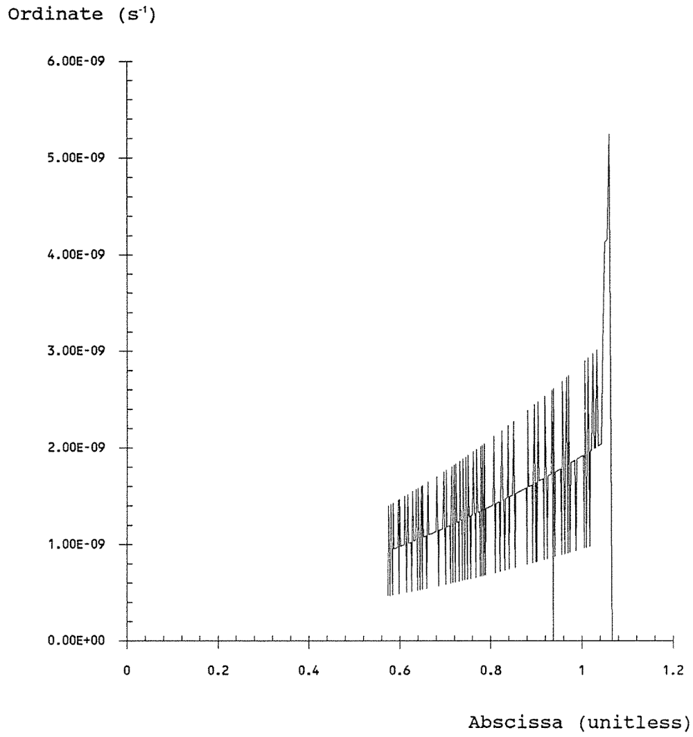
The Zerbst Plot Method of Parameter Calculation
The Zerbst plot can be used to extract the two thermal generation parameters described above for a specific device. The Zerbst plot is a way of presenting the capacitance versus time transient of a MOS capacitor as it decays without illumination from deep depletion to inversion. The Zerbst plot is a graph of the negative time derivative of (Co/C)2 against (CF/C -1) where CF is the final (equilibrium) capacitance which the MOS capacitor achieves during the transient. The ordinate of the Zerbst plot is proportional to the rate of thermal charge generation and the abscissa is proportional the depletion layer depth. Assuming the linear model of charge generation, the Zerbst plot is linear. In practice the model ceases to hold as the depletion layer approaches its equilibrium depth but is generally relatively linear for large values of the abscissa. If the linear part of the graph is extrapolated back to the ordinate, then τ is inversely proportional to the slope and s is directly proportional to the intercept.
A MOS capacitor's depletion layer depth can be calculated from its capacitance. Assuming the linear model of charge generation, Zerbst plot data can be used to calculate dQ/dt as a function of time and thus charge as a function of time. However, it is shown in Equation 6-8 that there is a more direct method of calculating charge versus time which does not depend on the validity of the linear model. For this reason, the Zerbst plot should not be used for this purpose but should only be used to extract the two parameters which are commonly used to describe the thermal generation properties (and hence quality) of a MOS capacitor and the semiconductor it is built on.
Test of Validity for Charge Generation Model
It is desirable to test the validity of the charge generation model (Equation 6-4) for a MOS capacitor under optical illumination. Since it is possible to measure the capacitance versus time transient of a MOS capacitor under optical illumination and it is possible to calculate the charge versus time transient from this data (Equation 6-7), it should be possible to substitute measurable variables (Equation 6-2) into the charge generation model and verify that it yields an expression which accurately describes a measured capacitance versus time transient. If measurable variables are substituted into this equation, then the expression in Equation 6-11 results. This can be discretized in the manner of Equation 6-8 to use data sets acquired with the capacitance meter.
One way to test the validity of the charge generation model is to measure a capacitance versus time transient, perform the operation defined by the right hand side of Equation 6-11, and verify that it is in fact constant. Assuming that it is constant, Equation 6-11 provides a means to use a capacitance versus time transient measured while under a known illumination to calculate the quantum efficiency of a MOS capacitor which is corrected for thermal generation.
Chapter 7
CHARACTERIZATION OF A TEST STRUCTURE INTEGRATED CIRCUIT
Doping Profile Calculations
To calculate the doping profiles for the MOS capacitors in the test structure IC, deep depletion capacitance versus voltage curves were required. A single n-type and a single p-type MOS capacitor were chosen for investigation. The properties measured for these two MOS capacitors are taken as representative of properties to be expected from MOSIS MOS capacitors in general.
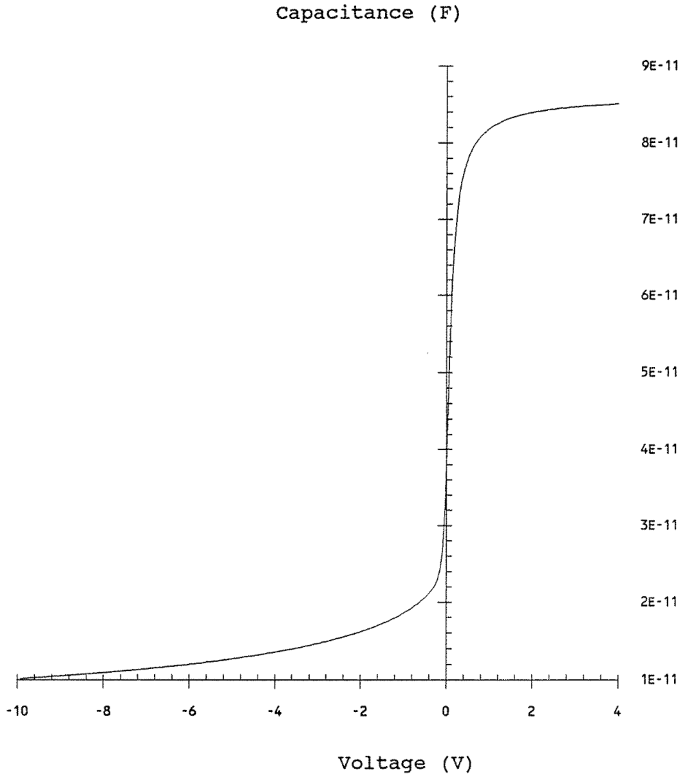
Deep depletion capacitance versus voltage measurements were made for these two MOS capacitors and doping profiles were calculated from this data using Equations 6-1 and 6-2. The deep depletion capacitance versus voltage response for the n-type MOS capacitor is presented in Figure 7-1. The response for the p-type MOS capacitor is presented in Figure 7-2. The doping profiles are presented in Figures 7-3 and 7-4.

Figures 7-3 and 7-4 present calculated doping profiles for bias voltages between 0 and 8 volts. This technique for calculating doping profiles becomes unreliable at very small bias voltages. Small bias voltages correspond to small depletion layers. Therefore, these profiles are not valid at small silicon depths.

The following are expected results. First, the p-well is more heavily doped than the substrate. This is typical for a p-well CMOS process. Second, for the same bias potential, the p-well does not develop as deep a depletion layer as does the substrate. Since the p-well is more heavily doped, at a given bias the depletion layer does not need to be as deep to move the same quantity of charge away from the gate.
The following are unexpected results. First, the measured dopant concentrations deviate significantly from the nominal values provided by MOSIS. MOSIS specifies the p-well doping to be 7.4x1015 cm-3 and the substrate doping to be 7.6x1015 cm-3. These values are only intended for use as fitting parameters to be used in MOS transistor simulation. They are not intended to be actual values and failure to measure these values is not a source of concern. Second, the substrate is expected to be uniformly doped and the measurements indicate that it is not. The p-well is doped by ion implantation and thermal diffusion. Thus, p-well doping levels are not expected to be constant. The calculated doping indicates that its doping is relatively uniform. Even disregarding the very shallow data points, both profiles appear to show some buildup (retrograde doping) with depth and the p-well doping is more uniform than the substrate.
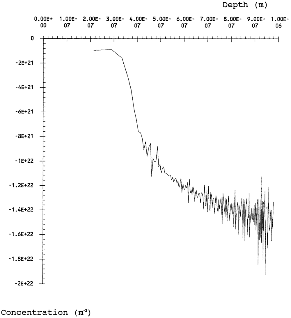
Since the calculated values of doping appear to approach an asymptotic value for relatively large values of W, these asymptotic values are taken as being the meaningful values. This approximation is conservative since it will overestimate the thermal generation parameters. When these parameters are used to compensate quantum efficiency measurements, it will cause the quantum efficiency to be underestimated. These values were graphically measured from figures 7-3 and 7-4. The doping level (N) of the substrate is -1.50x1016 cm-3 and the doping level of the p-well is +2.45x1016 cm-3. The sign of the doping level implies the sign of the charge carriers contributed by the dopant atom.
The difference in doping concentrations and thus achievable depletion layer depth establishes a tentative precedence between the n-type and p-type MOS capacitors for use as a sensor element. The mean penetration depth of 540 nm photons in silicon is somewhere between 1 and 2 μm9 and photon flux decreases exponentially with depth. Since the deep depletion layers formed had depths of up to 1 μm, maximizing depletion layer depth is expected to be a significant issue for good quantum efficiency. Since the n-type MOS capacitor is able to form deeper depletion layers, it is tentatively the preferred sensor element. Additionally, charge carriers have greater mobility in more lightly doped materials8 making them easier to collect. This is also a factor in favor of the n-type MOS capacitor. As a preparation for the possibility that thermal generation becomes the limiting factor in device performance, the thermal generation properties of both MOS capacitor types will be evaluated. However, since quantum efficiency is expected to be the limiting factor and is certainly the most crucial factor, it will only be measured for the n-type MOS capacitor.
Zerbst Plot Calculation
To create Zerbst plots for these MOS capacitors, capacitance versus time transients were measured at room temperature (80˚ F) while the IC was shielded from illumination. No correction was made for the parasitic capacitance of the IC package and on-chip wiring but these effects should be negligible. These data are plotted in Figures 7-5 and 7-6. From these data, Zerbst plots are calculated for the MOS capacitors as described in chapter 6 and these plots are presented in Figures 7-7 and 7-8. The slope and intercept were graphically measured from these plots for use in calculating material parameters.

The following data are needed in calculating material parameters from Zerbst plots:
The dopant concentrations were calculated in the last section. The permittivity of silicon7 (ε) is the product of the permittivity of free space and the dielectric constant of silicon. Another quantity which is needed is the intrinsic carrier concentration (ni) of silicon. This term is only temperature dependent. At the measurement temperature, the value of ni is 2x10¹⁶ m-3.
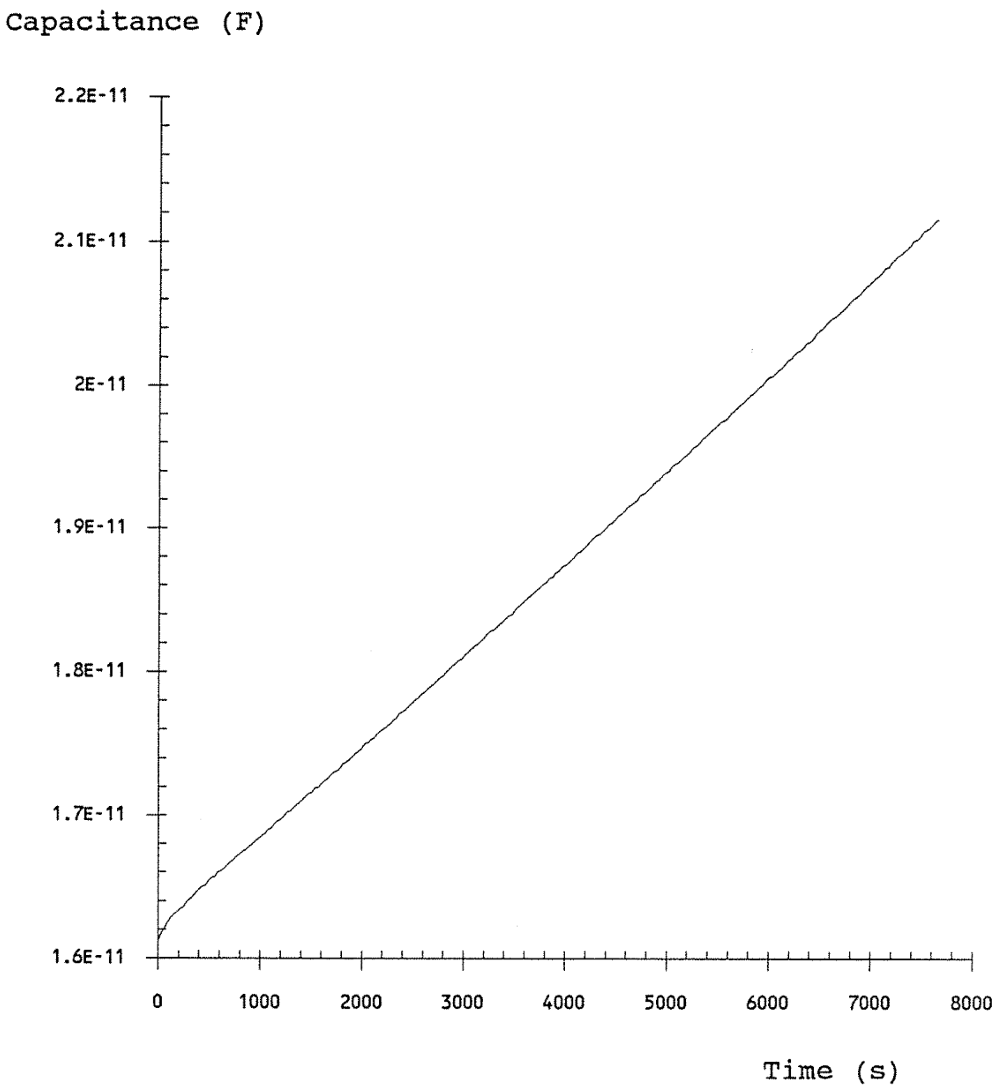
The complete capacitance versus time transient was measured as the n-type MOS capacitor decayed from deep depletion to inversion. It took approximately fifty minutes. This is quite long indicating high quality manufacturing. The calculated Zerbst plot represents this complete data set and is of approximately the expected shape. The noise seen in the Zerbst plot is not unexpected due to the small capacitance values measured. Graphically fitting a line to the linear (central) part of the curve yields the following values:
From the deep depletion capacitance versus voltage response (Figure 7-1), the oxide capacitance (Co) was measured to be 8.5x10⁻¹¹ F. From the thermal capacitance versus time transient, the final equilibrium capacitance (CF) was measured to be 2.0x10⁻¹¹ F. From these values, the thermal charge generation parameters were calculated using Equations 6-9 and 6-10 and are as follows:
The capacitance versus time transient measurement for the p-type MOS capacitor is not complete. Instrument problems prevented acquisition and storage of data for much longer than two hours and therefore only partial data was collected. Once again, a transient of this length indicates a device of very high quality. As can be seen in Figure 7-8, the Zerbst plot calculated from this incomplete data set is also incomplete. It appears in this graph that a very smooth curve is being traced out with intermittent spikes in the positive and negative directions. These fluctuations are probably caused by the uncertainty of the last significant figure of the measurement of the capacitance by the CV-590 meter. The best fit line to this graph has a negative intercept. This is inconsistent with the thermal generation model. Closer scrutiny of this graph shows that it is nonlinear and has a positive second derivative. To evaluate the material parameters, an intercept of zero is assumed and the slope was measured graphically by connecting a straight line between the origin and the approximate centroid of the available graph. This introduces significant error but it is clear that the linear model of thermal generation is only a crude approximation for this device. The results obtained using this method are:
From the deep depletion capacitance versus voltage response, Co was measured to be 8.2x10⁻¹¹ F. Using the oxide thickness provided by MOSIS, the expected oxide capacitance is 8.6x10⁻¹¹ F. The value of CF was not measured from the dark capacitance versus time transient because the complete transient was not measured. However, the equilibrium capacitance values of this MOS capacitor were measured at voltages near the bias used for this measurement (8 V). This was done by pulsing the MOS capacitor with light, waiting 30 seconds for it to recover, and then measuring capacitance. For biases near 8 V, the equilibrium capacitance was measured to be approximately 3.3x10⁻¹¹ F. For biases in this range, the final capacitance is not sensitively dependent on bias and can be measured reliably. Therefore this value is taken to be the value of CF. From these values, the thermal charge generation parameters were calculated and are:
Because the transient time of the p-type MOS capacitor is so long, considerations otherwise ignored might be important (e.g. extremely low level light leakage, temperature fluctuations, and background radiation levels). In addition, complete Zerbst plot data is not available and non-linearities are apparent. It can be said with certainty that thermal generation in the p-well is very slow and is significantly slower than in the substrate. Since thermal generation is a source of error signal in the system under consideration, this is a factor in favor of the p-type MOS capacitor. As described in Equation 6-11, these parameters can be used to correct quantum efficiency calculations for either of these MOS capacitors. Since the values of these parameters are very small, under normal circumstances, thermal generation is likely to represent only very small contributions.
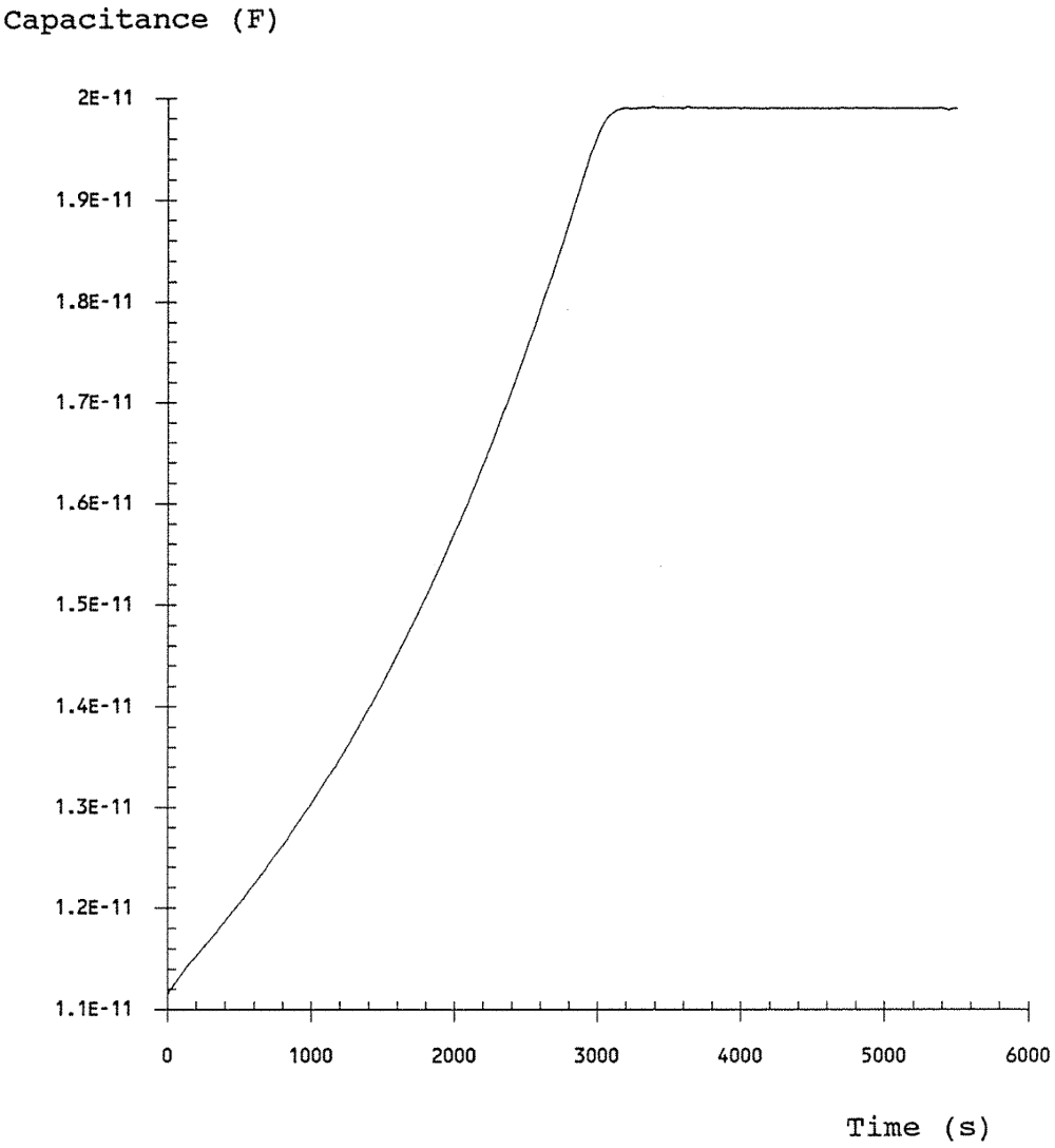
Measured Latitude
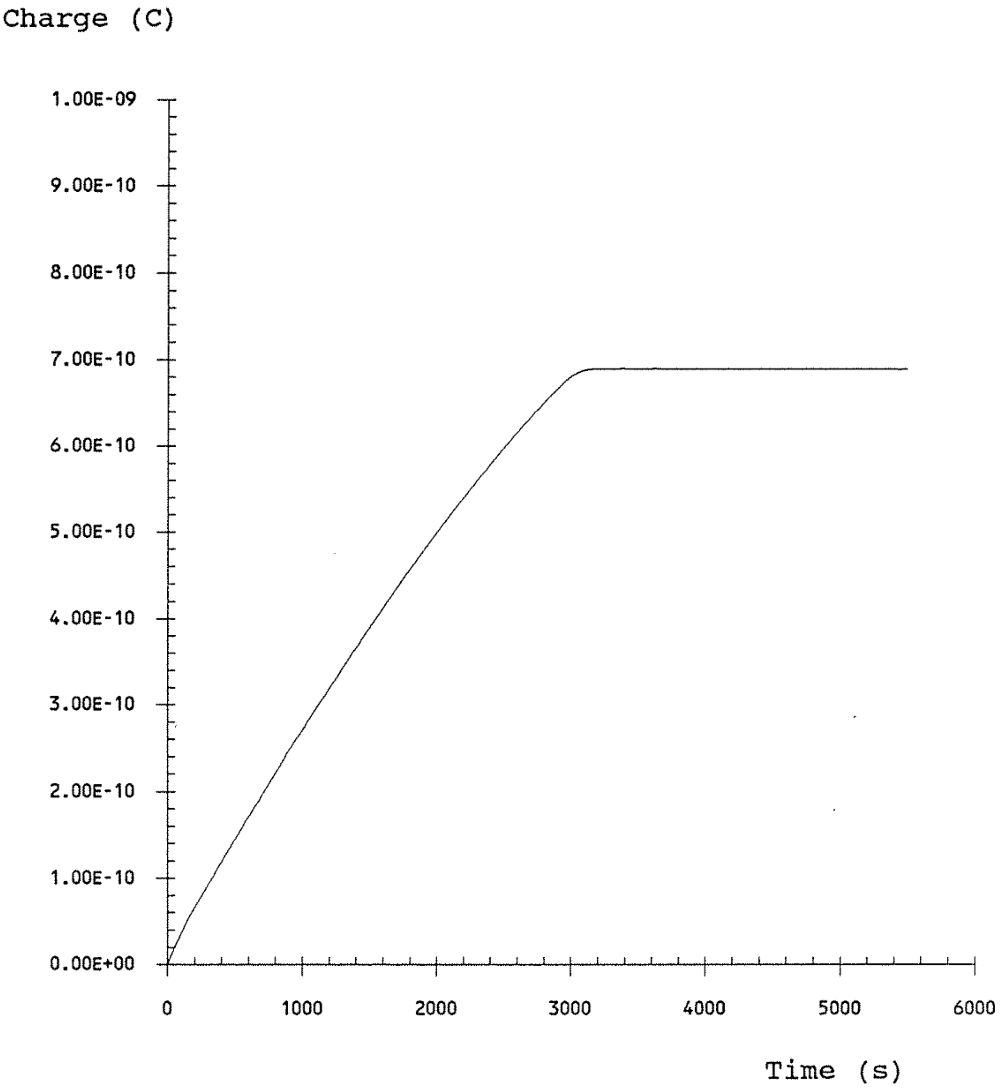
Equation 6-8 was used to convert the thermal capacitance versus time transient of Figure 7-1 into a charge versus time transient which is shown in Figure 7-9. It can be seen in Figure 7-9 that at equilibrium at 8 V, this MOS capacitor can hold a charge of approximately 6.8x10⁻¹⁰ C. The shape of the MOS capacitor is square with a side length of 330 μm. If a fill factor of 75% were achieved at 5 mm-1 resolution then this charge would be scaled (assuming it can be linearly scaled) to 4.7x10⁻¹¹ C. Using the assumptions for high end performance discussed in Chapter 4, a captured x-ray photon gives rise to 1559 optical photons which are incident on active sensor area. From Chapter 2, an average of 10.9x10⁶ x-ray photons are incident per square cm. This implies 818 x-ray photons incident in a 100 μm sensor element. If all of these are captured and converted to useful light and if the MOS capacitor has a 100% quantum efficiency for optical photons, then 1.3x10⁶ charges will be created. This corresponds to 2.0x10⁻¹³ C or less than 0.03% of the available latitude of the device. In other words the device is able to sense a much stronger illumination than is required. Available latitude does not limit the feasibility of the device being considered.
Quantum Efficiency at 540 nm
As already described, the principal optical photon being considered has a wavelength of 540 nm. Using the tungsten filament source and spectrometer, the MOS capacitor was illuminated with light of wavelength 540 nm at an intensity of 0.033 W/m2. This corresponds to a photon flux of 9.07x10¹⁶ m-2s-1. To protect the MOS capacitors on the IC, a thin glass cover slip was placed over the IC package opening. The air to glass interface seen by the incident field represents a reflectance in the system. A typical reflectance value for this type of interface in this range of wavelengths is approximately 8%i and thus the photon flux at the MOS capacitor surface is determined to be 8.35x10¹⁶ m-2s-1. The capacitance versus time transient was measured under this illumination and is shown in Figure 7-10. The time dependence of the quantum conversion efficiency was calculated using Equation 6-11 and is shown in Figure 7-11. This curve is relatively flat across most of its range and the value of quantum conversion efficiency for the early part of the range is measured to be 7%.
Note that the ripples seen in this graph are not due to the random uncertainty of individual data points. The fluctuations are periodic and have a frequency of approximately 1 Hz. The light source used for this measurement was a slide projector. Since the bulb was operated at a high power, a cooling fan was used. Since the MOS capacitor was not shielded against electromagnetic interference, this periodic noise was likely caused by the cooling fan. However, the oscillations are centered around 7% quantum efficiency. Note also, that toward the end of the measurement, the model is invalid, and the calculated quantum efficiency becomes very large.

Chapter 8
CONCLUSION AND RECOMMENDATIONS
Conclusion
The sensor which has been discussed is that of an array of MOSIS MOS capacitors, set on 100 μm centers, with a 75% fill factor. A plane of readout circuits faces the sensor array and a phosphor is sandwiched between them. The phosphor's properties lie somewhere between those of the Kodak Lanex - Regular screen and an idealized CsI(Tl) needle array. To perform in medical radiography, the objective is to resolve 40 keV photons. Based upon the discussion in Chapter 4, each absorbed 40 keV photon is expected to give rise to between 1188 and 1559 optical photons. In Chapter 7, a quantum efficiency of 7% was measured for a test structure MOS capacitor. Using this device, between 83 and 109 electrons could thus be expected from each x-ray photon. This represents an extremely small charge and resolution of a charge of this size will require amplifiers of extremely high quality. It is unlikely that such amplifiers can be implemented in the space constraints of this sensor.
Disparity Between Measured and Tabulated Quantum Efficiencies
Optical Quantum Efficiency
As discussed in Chapter 4, at the wavelength of interest a quantum efficiency of approximately 44% is expected for polysilicon gate MOS capacitors yet only a 7% quantum efficiency was measured for the test structure MOS capacitor. To keep capacitance measurements relatively noise-free, the test structure MOS capacitor was made with very large dimensions. The large capacitance value reduces uncertainties in its measurement. The gate of the MOS capacitor is made of polysilicon which is quite reflective and absorptive to optical photons. The gate is surrounded by relatively transparent silicon dioxide. In disagreement with the delta depletion approximation, the depletion layer does extend laterally beyond the edge of the gate. In addition, lateral diffusion can cause ehps to be detected which were not created in the shadow of the gate (which can lead to a deterioration of MTF). Therefore, a very sensitive sensor region is expected to exist around the edge of the MOS capacitor. Small squares or rectangles have more perimeter per unit area than do large ones and thus are expected to be more sensitive. The test structure MOS capacitors used have approximately 1000 times the area of typical CCD MOS capacitors and approximately 15 times the area of the projected sensor element MOS capacitor.
Response Function
As described in Chapters 3 and 4, good MOS capacitor quantum efficiency is expected to depend upon optical energy being deposited in or near the depletion layer and the only expected deviation from an ideal fluence detector model is some loss of sensitivity during an exposure cycle. The mean penetration depth of 540 nm photons is comparable to the maximum depletion layer depth of the n-type MOS capacitor at a bias of 8 V. The mean penetration depth is between 1 and 2 μm. Since no optically diffusing materials were placed between the light source and the sensor and the light source was located far from the sensor, normal incidence of photons is assumed and thus no off-axis adjustments are needed. Using Figure 7-5 and Equation 6-2, the initial and final depletion layer depths can be calculated for an optical exposure cycle. During an exposure, the depletion layer depth decreases from 0.93 μm to 0.30 μm so a significant portion of the photon energy is deposited beyond the depletion layer. If the depletion layer is the only sensitive region and diffusion is not an important effect, the sensitive volume is seen to decrease by a factor of three during a charging cycle and the sensitivity should decrease by a factor of three. However, this is not observed in Figure 7-11. The quantum efficiency remains essentially constant. This implies that diffusion is an important process in detection and that the same portion of generated carriers reach the depletion region independent of its depth. Essentially, carriers are able to diffuse at least one or two μm after generation to be detected. Part of the justification for neglecting p-type MOS capacitor is that n-type capacitors are able to form deeper depletion layers. Since quantum efficiency has been shown to not be sensitively dependent on depletion layer depth, this issue should be re-evaluated.
Methods of Improving Optical Quantum Efficiency
Inherent Differences
Based on the arguments of the last section, the quantum efficiency of a MOS capacitor of the proposed size may be better than the calculations of Chapter 7 indicate. This is due to an enhanced perimeter effect for smaller MOS capacitors. In addition, the proposed geometry includes a close-coupling of a phosphor layer with a MOS capacitor. The measured quantum efficiency was for optical photons incident from air. If the photons enter the MOS capacitor from a phosphor layer, a smaller reflectance will be created due to a closer matching of the refractive index of these contacting layers. This would also improve the quantum efficiency of the proposed system.
The measurement was made with a relatively planar beam whereas a close-coupled phosphor will create a light field which is non-planar. Optical photons which strike an interface at non-normal incidence are more likely to be reflected thus creating an apparent reduction in quantum efficiency. However if a CsI(Tl) needle structure (effectively a waveguide array) can be used, a generally forward direction of optical photon travel can be retained and this consideration will be minimized.
Design Variations
As described in Chapter 4, use of a transparent gate material such a tin oxide can significantly increase the quantum efficiency of a MOS capacitor. In general, prudent choice of MOS capacitor layer materials and thicknesses can function as an anti-reflective coating and lead to decreased reflectance causing an increased quantum efficiencyi. In the absence of transparent gate materials, windows can be created in the poly gate layer through which light can pass thus improving the quantum efficiency11. Diffusion seems to be an important process in the detection of charge carriers. For this reason, it may be possible to place large windows in a sensor element without any significant loss of collection efficiency.
Another test structure IC containing MOS capacitors has been fabricated. It has not been completely characterized. When illuminated by white light, however, a square MOS capacitor whose side length is 25 μm takes significantly less time to equilibrate at than does one whose side length is 330 μm. Assuming a capacitive charge storage ability which is normalized to area, a smaller time to equilibrate under a constant illumination implies a greater quantum efficiency. In addition, two test structure MOS capacitors (each a 100 μm square) were fabricated on the IC. The only difference in their structure is that the polysilicon gate of one has an array of perforations (filled with transparent thick silicon dioxide) across its surface. This MOS capacitor is referred to as a fishnet capacitor. When exposed to white light, the fishnet capacitor equilibrates much more rapidly than does its unperforated counterpart. This implies that such a design might be used to optimize the quantum efficiency of a MOS capacitor sensor element.
Further Suggested Work
Investigating Thermal Generation
Thermal generation is a source of signal error for the proposed system. Though thermal generation was very slow for the test structure IC, it was still present. In addition, its contribution is expected to increase1 with accumulated dose. Thermal generation's contribution can be removed by subtracting an unilluminated exposure from an acquired image. Some attempt should be made to evaluate thermal generation in the context of image noise to determine how significant its contribution is, how much is acceptable, how it can best be minimized. In addition, the effect of sensor element geometry on thermal generation should be evaluated.
Modeling and Simulating
How a MOS capacitor is designed and operated impacts the depletion layer (sensor) it forms. Different types of phosphor layers will interact differently with different MOS capacitor designs. A CsI(Tl) needle array will create a different type of optical field than a layer of Gd2O2S(Tb) which is suspended in a lucite matrix and laid over the MOS capacitor. It would be desirable to model and simulate the detection process of the MOS capacitor/phosphor system to determine how to build the optimal sensor element. It would be ideal to model the entire image sensing process: x-ray transport in the phosphor and MOS capacitor, light transport in the phosphor and into the MOS capacitor, charge generation, charge transport, and charge collection. In addition to the varying reflectance across the surface of the MOS capacitor, the actual (non-idealized) geometry of the depletion layer must be considered as well as the diffusion properties of the silicon wafer and the effect of substrate contacts. To evaluate the properties of the MOS capacitors fabricated with a given process, an isolated MOS capacitor on a wafer can be pulse illuminated by a highly focused laser and the resulting charge generation measured. If this is repeated as a function of position over the MOS capacitor and the wafer and, it is anticipated that the diffusion properties can be determined from these measurements. This information can then be used for modeling and simulation. If work is to continue on development of the MOS capacitor for use in digital radiography, careful modeling of its optical and electrical properties is the most important next step.
Reference List
- Jacobs, A.M., Cox, J.C., and Juang, Y.S., "DRAM as an X-Ray Sensor", Proceedings of SPIE, 797, 124-126, 1987.
- Johns, H.E. and Cunningham, J.R., The Physics of Radiology, 234-235, (Bannerstone House, Springfield, IL, 1974)
- Rose, A., Vision, Human and Electronic, 20-22, (Plenum Press, New York, 1973)
- Barrett and Swindell, Radiological Imaging, The Theory of Image Formation, Detection, and Processing, Volume I, 236-239, (Academic Press, New York, 1981)
- Society for Non-Destructive Testing, Nondestructive Testing Handbook, Volume 3, 598, (American Society for NonDestructive Testing, USA, 1985)
- Knoll,G. F., Radiation Detection and Measurement, 231, (John Wiley and Sons, New York, 1979)
- Schroder, D.K., Advanced MOS Devices, 45-147, (Addison-Wesley Publishing Company, Reading, MA, 1987)
- Pierret R.F., Semiconductor Fundamentals, 47-60, (Addison-Wesley Publishing Company, Reading, MA, 1983)
- Sze, S.M., Semiconductor Devices, Physics and Technology, 257, (John Wiley and Sons, New York, 1985)
- Melles Griot, Optics Guide 4, 3-4, (Melles Griot, New York, 1988)
- Weijtens, C.H.L., Keur, W.C., "Reduction of Reflection Losses in Solid State Image Sensors", Proceedings of SPIE, 591, 75, 1985.
Biographical Sketch
Robert Paul King, Jr. was born in Jacksonville, Florida, in 1964. He graduated from S.W. Wolfson High School and entered service in the U.S. Army in 1982. He enrolled at the University of Florida in January of 1986 and was awarded the degree of Bachelor of Science in electrical engineering in December of 1988. He enrolled in the medical physics program in the Department of Nuclear Engineering Sciences in January of 1989 and has worked for the Master of Science degree until the present.
I certify that I have read this study and that in my opinion it conforms to acceptable standards of scholarly presentation and is fully adequate, in scope and quality, as a thesis for the degree of Master of Science.
Alan M. Jacobs, Chair
Professor of Nuclear Engineering Sciences
I certify that I have read this study and that in my opinion it conforms to acceptable standards of scholarly presentation and is fully adequate, in scope and quality, as a thesis for the degree of Master of Science.
David E. Hintenlang
Assistant Professor of Nuclear Engineering Sciences
I certify that I have read this study and that in my opinion it conforms to acceptable standards of scholarly presentation and is fully adequate, in scope and quality, as a thesis for the degree of Master of Science.
Robert M. Fox
Assistant Professor of Electrical Engineering
I certify that I have read this study and that in my opinion it conforms to acceptable standards of scholarly presentation and is fully adequate, in scope and quality, as a thesis for the degree of Master of Science.
Walter E. Drane
Associate Professor of Radiology
I certify that I have read this study and that in my opinion it conforms to acceptable standards of scholarly presentation and is fully adequate, in scope and quality, as a thesis for the degree of Master of Science.